DATA SHEET
www.onsemi.com MOSFET – Single, N-Channel,
POWERTRENCH),
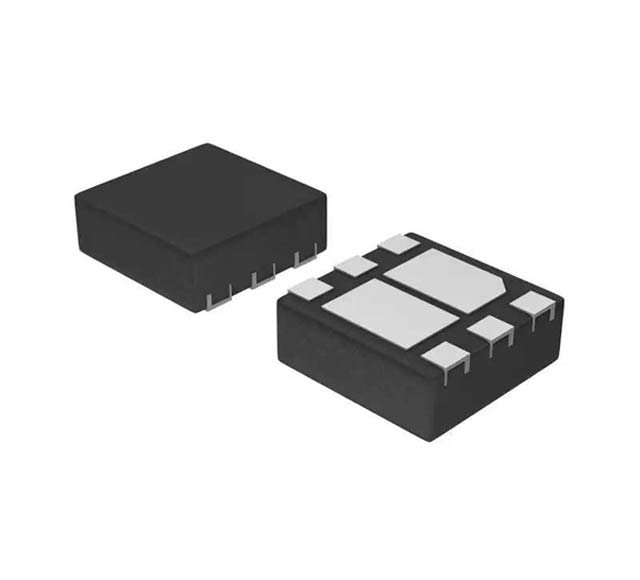
2.5 V Specified VDS RDS(on) MAX ID MAX 30 V 40 mW @ 4.5 V 5.0 A 50 mW @ 2.5 V 30 V, 5.0 A, 40 mW Pin 1 FDMA430NZ D D G Source Drain General Description This Single N−Channel MOSFET has been designed using
onsemi’s advanced POWERTRENCH process to optimize
the RDS(on) @ VGS = 2.5 V on special MicroFETt leadframe. D S
Bottom Features • RDS(on) = 40 mW at VGS = 4.5 V, ID = 5.0 A
• RDS(on) = 50 mW at VGS = 2.5 V, ID = 4.5 A
• Low Profile − 0.8 mm Maximum in the New Package MicroFET
•
•
• D WDFN6 2x2, 0.65P
(MicroFET 2x2)
CASE 511CZ 2x2 mm
HBM ESD Protection Level > 2.5 kV Typical (Note 3)
Free from Halogenated Compounds and Antimony Oxides
This Device is Pb−Free, Halide Free and is RoHS Compliant MARKING DIAGRAM &Z&2&K
430 Applications • Li−lon Battery Pack
ABSOLUTE MAXIMUM RATINGS (TA = 25°C, unless otherwise noted)
Parameter Symbol Ratings Unit VDSS Drain−Source Voltage 30 V VGSS Gate−Source Voltage ±12 V ID Drain Current
− Continuous (Note 1a)
− Pulsed PD Power Dissipation (Steady State)
− (Note 1a) …