Datasheet JX Semiconductor ASC40N1700MT3 — 数据表
| 制造商 | JX Semiconductor |
| 系列 | JX3S0040170M |
| 零件号 | ASC40N1700MT3 |
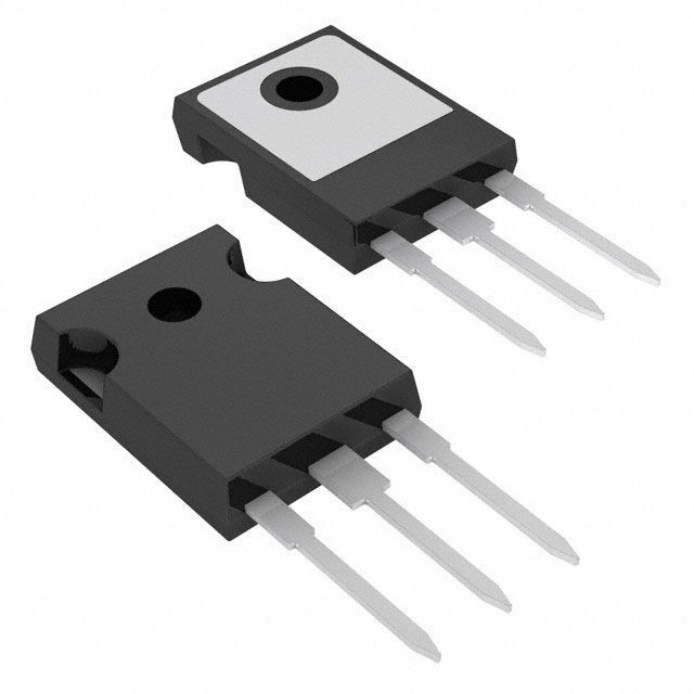
1700V、40A、72mΩ、N沟道、碳化硅MOSFET,采用TO-247-3L封装
数据表
1700V, 40A, 72mΩ, N-Channel, Silicon Carbide MOSFET in TO-247-3L package
JX3S0040170M 1700V, 40A, 72mΩ, N-Channel, Silicon Carbide MOSFET
Product Data Sheet JX-3T04-40A A/2 General Description
TheJX-MT3 series SiC MOSFET in TO-247-3L package
ensures stable high-temperature operation for power-dense
and energy-critical systems, enabling compact designs with
reduced EMI. Features 3rd Generation SiC MOSFET Technology High-Speed Switching with Low Capacitances High Blocking Voltage with Low RDS(on) Easy to Parallel and Simple to Drive RoHS Compliant, Halogen Free Ordering Informations Applications EV Motor Drive High Voltage DC/DC Converters Switch Mode Power Supplies Solar Inverters
EV Charging Order Number ASC40N1700MT3 Marking ASC40N1700MT3 Package Type TO-247-3L Packing Method Tube Key Parameters
Symbol Parameter Values Unit Test Conditions 1700 V TC=25°C Absolute maximum rating
VDS Drain-Source Voltage ID Drain Current (Continuous) 40 A TC=25°C PD Power Dissipation 242 W TC=25OC TJ Junction Temperature 175 OC Symbol Parameter Min. Typ. Max. -72 88 -130 -Unit Test Conditions Static characteristics
RDS(on) Static Drain-Source on Resistance mΩ VGS=18V; ID=20A; TJ=25°C
VGS=18V; ID=20A; TJ=175°C Dynamic characteristics
QG Total Gate Charge -100 -QGD Gate-Drain Charge -22 -360 -nC VDS=1000V; VGS=-5/+18V; ID=25A;
TJ=25°C nC VGS=-5V; IF=20A; VR=1000V;
di/dt=1000A/μs; TJ=175°C Source-drain diode
Qrr Reverse Recovery Charge Product Data Sheet 1 JX-3T04-40 AA/2 JX3S0040170M 1700V, N-Channel, Silicon Carbide MOSFET Absolute Maximum Ratings (at TC=25 °C unless otherwise specified)
Symbol Values Unit 1700 V Drain Current (Continuous; TC=25OC) 40 A Drain Current (Continuous; TC=100OC) 28 A IDM Drain Current (Pulsed) 118 A VGS Gate-Source Voltage -10/+22 V PD Power Dissipation 242 W -55 to +175 OC VDS
ID TJ ; Tstg Parameter
Drain-Source Voltage Junction and Storage Temperature Range MOSFET Characteristics
Symbol Parameter Min. Typ. Max. Unit Test Conditions Static characteristics (at TJ=25°C unless otherwise specified)
BVDS Drain-Source Breakdown Voltage 1700 -V ID=250μA; VGS=0V IDSS Zero Gate Voltage Drain Current -5 100 μA VDS=1700V; VGS=0V IGSS Gate-Body Leakage Current -10 150 nA VGS=-10 to 20V; VDS=0V VGS(th) Gate Threshold Voltage 2 3 4 V VDS=VGS ; ID=10mA VGS(on) Recommended Turn-on Voltage -18 -VGS(off) Recommended Turn-off Voltage -5 -V Static RDS(on) Static Drain-Source on Resistance -72 88 -130 -mΩ VGS=18V; ID=20A; TJ=25OC
VGS=18V; ID=20A; TJ=175OC Dynamic characteristics (at TJ=25°C unless otherwise specified)
Ciss Input Capacitance -2450 -Coss Output Capacitance -90 -Crss Reverse Transfer Capacitance -3 -gfs Transconductance -1 …
1700V, 40A, 72mΩ, N-Channel, Silicon Carbide MOSFET in TO-247-3L package
JX3S0070R170M 1700V, 40A, 72mΩ, N-Channel, Silicon Carbide MOSFET General Description
The JX-MT3 series SiC MOSFET in TO-247-3L package
ensures stable high-temperature operation for power-dense
and energy-critical systems, enabling compact designs with
reduced EMI. Features 3rd Generation SiC MOSFET Technology High-Speed Switching with Low Capacitances High Blocking Voltage with Low RDS(on) Easy to Parallel and Simple to Drive RoHS Compliant, Halogen Free Ordering Informations Applications EV Motor Drive High Voltage DC/DC Converters Switch Mode Power Supplies Solar Inverters
EV Charging Order Number ASC40N1700MT3 Marking ASC40N1700MT3 Package Type TO-247-3L Packing Method Tube Key Parameters
Symbol Parameter Values Unit Test Conditions 1700 V TC=25°C Absolute maximum rating
VDS Drain-Source Voltage ID Drain Current (Continuous) 40 A TC=25°C PD Power Dissipation 242 W TC=25OC TJ Junction Temperature 175 OC Symbol Parameter Min. Typ. Max. -72 88 -130 -Unit Test Conditions Static characteristics
RDS(on) Static Drain-Source on Resistance mΩ VGS=18V; ID=20A; TJ=25°C
VGS=18V; ID=20A; TJ=175°C Dynamic characteristics
QG Total Gate Charge -100 -QGD Gate-Drain Charge -22 -360 -nC VDS=1000V; VGS=-5/+18V; ID=25A;
TJ=25°C nC VGS=-5V; IF=20A; VR=1000V;
di/dt=1000A/μs; TJ=175°C Source-drain diode
Qrr Reverse Recovery Charge Product Data Sheet 1 JXC-3T04-40 AA/2 JX3S0070R170M
1700V, N-Channel, Silicon Carbide MOSFET Absolute Maximum Ratings (at TC=25 °C unless otherwise specified)
Symbol Values Unit 1700 V Drain Current (Continuous; TC=25OC) 40 A Drain Current (Continuous; TC=100OC) 28 A IDM Drain Current (Pulsed) 118 A VGS Gate-Source Voltage -10/+22 V PD Power Dissipation 242 W -55 to +175 OC VDS
ID TJ ; Tstg Parameter
Drain-Source Voltage Junction and Storage Temperature Range MOSFET Characteristics
Symbol Parameter Min. Typ. Max. Unit Test Conditions Static characteristics (at TJ=25°C unless otherwise specified)
BVDS Drain-Source Breakdown Voltage 1700 -V ID=250μA; VGS=0V IDSS Zero Gate Voltage Drain Current -5 100 μA VDS=1700V; VGS=0V IGSS Gate-Body Leakage Current -10 150 nA VGS=-10 to 20V; VDS=0V VGS(th) Gate Threshold Voltage 2 3 4 V VDS=VGS ; ID=10mA VGS(on) Recommended Turn-on Voltage -18 -VGS(off) Recommended Turn-off Voltage -5 -V Static RDS(on) Static Drain-Source on Resistance -72 88 -130 -mΩ VGS=18V; ID=20A; TJ=25OC
VGS=18V; ID=20A; TJ=175OC Dynamic characteristics (at TJ=25°C unless otherwise specified)
Ciss Input Capacitance -2450 -Coss Output Capacitance -90 -Crss Reverse Transfer Capacitance -3 -gfs Transconductance -16 Eoss Coss Stored Energy -Eon …
详细说明
JX-MT3 系列 SiC MOSFET 采用 TO-247-3L 封装,可确保高功率密度和高能耗系统在高温下稳定运行,从而实现紧凑设计并降低 EMI。
模型线
- ASC40N1700MT3 JX3S0040170M
制造商分类
- Silicon Carbide Metal-Oxide-Semiconductor Field-Effect Transistor