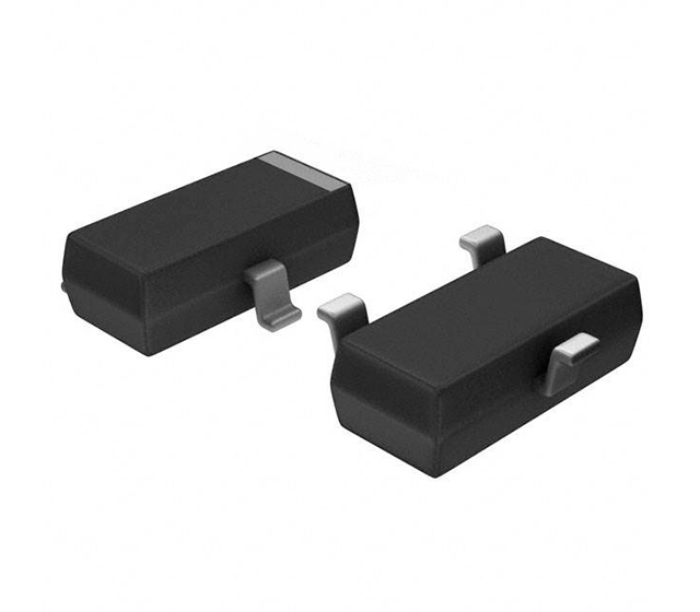
PDF, 244 Kb, 语言: en, 文件上传: Jul 27, 2026, 页数: 12
N-channel TrenchMOS ultra low level FET in SOT23 package
从文件中提取
PMV30UN
µTrenchMOS™ ultra low level FET
Rev. 01 — 25 June 2003 Product data M3D088 1. Product profile
1.1 Description
N-channel enhancement mode field-effect transistor in a plastic package using
TrenchMOS™ technology.
Product availability:
PMV30UN in SOT23. 1.2 Features
■ Surface mount package ■ Fast switching. 1.3 Applications
■ Battery management ■ High-speed switches. 1.4 Quick reference data
■ VDS ≤ 20 V
■ Ptot ≤ 1.9 W ■ ID ≤ 5.7 A
■ RDSon ≤ 36 mΩ 2. Pinning information
Table 1: Pinning -SOT23 simplified outline and symbol Pin Description 1 gate (g) 2 source (s) 3 drain (d) Simplified outline Symbol
d 3 g 1 2 Top view SOT23 MSB003 MBB076 s PMV30UN Philips Semiconductors µTrenchMOS™ ultra low level FET 3. Limiting values
Table 2:
Limiting values
In accordance with the Absolute Maximum Rating System (IEC 60134).
Symbol Parameter Conditions Min Max Unit VDS drain-source voltage (DC) 25 °C ≤ Tj ≤ 150 °C -20 V VDGR drain-gate voltage (DC) 25 °C ≤ Tj ≤ 150 °C; RGS = 20 kΩ -20 V VGS gate-source voltage (DC) -±8 V ID drain current (DC) Tsp = 25 °C; VGS = 4.5 V; Figure 2 and 3 -5.7 A Tsp = 100 °C; VGS = 4.5 V; Figure 2 -3.65 A IDM peak drain current Tsp = 25 °C; pulsed; tp ≤ 10 µs; Figure 3 -23.1 A Tsp = 25 °C; Figure 1 Ptot total power dissipation -1.9 W Tstg storage temperature −55 +150 °C Tj junction temperature −55 +150 °C Source-drain diode
IS source (diode forward) current (DC) Tsp = 25 °C -1.6 A ISM peak source (diode forward) current Tsp = 25 °C; pulsed; tp ≤ 10 µs -6.4 A © Koninklijke Philips Electronics N.V. 2003. All rights reserved. 9397 750 11569 Product data Rev. 01 — 25 June 2003 2 of 12 PMV30UN Philips Semiconductors µTrenchMOS™ ultra low level FET 03aa17 120 03aa25 120
Ider
(%) Pder
(%) …