PDF, 267 Kb, 语言: en, 文件上传: Nov 26, 2025, 页数: 6
Small Signal JFET N-Channel in TO-92 package
从文件中提取
MPF4392, MPF4393
JFET Switching Transistors
N−Channel − Depletion
Features Pb−Free Packages are Available* http://onsemi.com
2 SOURCE MAXIMUM RATINGS
Rating Symbol Value Unit Drain −Source Voltage VDS 30 Vdc Drain −Gate Voltag VDG 30 Vdc Gate−Source Voltage VGS 30 Vdc Forward Gate Current IG(f) 50 mAdc Total Device Dissipation
@ TA = 25C
Derate above 25C PD 350
2.8 mW
mW/C −65 to +150 C Operating and Storage Channel
Temperature Range Tchannel,
Tstg Stresses exceeding Maximum Ratings may damage the device. Maximum
Ratings are stress ratings only. Functional operation above the Recommended
Operating Conditions is not implied. Extended exposure to stresses above the
Recommended Operating Conditions may affect device reliability. 3
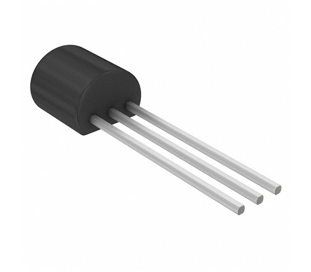
GATE 1 DRAIN 1 12 3
STRAIGHT LEAD
BULK PACK TO−92 (TO−226AA)
CASE 29−11
STYLE 5 2 3
BENT LEAD
TAPE & REEL
AMMO PACK MARKING DIAGRAM …