Datasheet Efficient Power Conversion EPC23101 — 数据表
| 制造商 | Efficient Power Conversion |
| 系列 | EPC23101 |
| 零件号 | EPC23101 |
100 V、65 A ePower 芯片组
数据表
ePower Chipset 100 V, 65 A
eGaN® FET DATASHEET EPC23101 EPC23101 – ePower™ Chipset
VIN , 100 V
ILoad , 65 A Y NAR
I
M
I
REL EFFICIENT POWER CONVERSION P HAL EPC’s ePowerTM Stage and Chipset integrate input logic interface, level shifting, bootstrap charging
and gate drive buffer circuits along with eGaN output FETs. Integration is implemented using EPC’s
proprietary GaN IC technology. The end result is a Power Stage that translates logic level input to
high voltage and high current power output that is smaller in size, easier to manufacture, simpler to
design and more efficient to operate. Key Parameters
PARAMETER VALUE UNIT Power Stage Load Current (1 MHz)
Operating PWM Frequency Range
Absolute Maximum Input Voltage
Operating Input Voltage Range
Nominal Bias Supply Voltage 65 [1] A
MHz 3 [2]
100
80
5 V Output Current and PWM Frequency Ratings are functions of Operating Conditions. Appropriate derating should be
applied to keep TJ at less than 125 °C. See Notes 1 & 2. Chipset Information
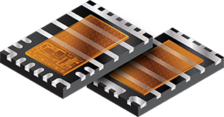
PART NUMBER Rated RDS(on) at 25°C QFN Package Size (mm) EPC23101 3.3 mΩ 3.5 x 5 EPC2302 1.8 mΩ 3x5 All exposed pads feature wettable flanks that allow side wall solder inspection. High voltage and low voltage pads
are separated by 0.6 mm spacing to meet IPC rules. Recommended to use EPC2302 as companion low side FET for …
Enhancement Mode Power Transistor 100 V, 1.8 mΩ max
eGaN® FET DATASHEET EPC2302 EPC2302 – Enhancement Mode Power Transistor
VDS , 100 V
RDS(on) , 1.8 mΩ max Y NAR
I
M
I
REL D
G EFFICIENT POWER CONVERSION P S HAL The EPC2302 is a 1.8 mΩ max RDS(on), 100 V eGaN® power transistor in a low inductance 3 x 5 mm QFN
package with exposed top for excellent thermal management. It is tailored to high frequency DC-DC
applications to/from 40 V–60 V and 48 V BLDC motor drives.
The thermal resistance to case top is ~0.2 °C/W, resulting in excellent thermal behavior and easy
cooling. The device features an enhanced PQFN “Thermal-Max” package. The exposed top enhances
top-side thermal management and the side-wettable flanks guarantee that the complete side-pad
surface is wetted with solder during the reflow soldering process, which protects the copper and
allows soldering to occur on this external flank area for easy optical inspection.
Compared to a Si MOSFET, the footprint of 15 mm2 is less than half of the size of the best-in-class Si
MOSFET with similar Rds(on) and voltage rating, QG and QGD are significantly smaller and QRR is 0.
This results in lower switching losses and lower gate driver losses. Moreover, EPC2302 is very fast
and can operate with deadtime less than 10 ns for higher efficiency and QRR = 0 is a big advantage
for reliability and EMI. In summary, EPC2302 allows the highest power density due to enhanced
efficiency, smaller size, and higher switching frequency for smaller inductor and fewer capacitors.
The EPC2302 enables designers to improve efficiency and save space. The excellent thermal behavior
enables easier and lower cost cooling. The ultra-low capacitance and zero reverse recovery of the …
详细说明
与 EPC2302 配对以形成高达 65 A 的功率级
集成半桥驱动器,电平转换,
自举和高边 FET
功率级负载电流 (1 MHz),65 A
最大输入电压,100 V
其他选择
制造商分类
- Gate Drivers