Datasheet Texas Instruments CD74ACT139 — 数据表
| 制造商 | Texas Instruments |
| 系列 | CD74ACT139 |
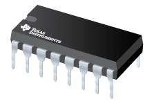
双2至4线路解码器/解复用器
数据表
状态
| CD74ACT139E | CD74ACT139EE4 | CD74ACT139M | CD74ACT139M96 | CD74ACT139M96E4 | CD74ACT139M96G4 | CD74ACT139ME4 | CD74ACT139MG4 | |
|---|---|---|---|---|---|---|---|---|
| Lifecycle Status | Active (Recommended for new designs) | Active (Recommended for new designs) | Active (Recommended for new designs) | Active (Recommended for new designs) | Active (Recommended for new designs) | Active (Recommended for new designs) | Active (Recommended for new designs) | Active (Recommended for new designs) |
| Manufacture's Sample Availability | No | No | No | No | No | No | No | No |
打包
| CD74ACT139E | CD74ACT139EE4 | CD74ACT139M | CD74ACT139M96 | CD74ACT139M96E4 | CD74ACT139M96G4 | CD74ACT139ME4 | CD74ACT139MG4 | |
|---|---|---|---|---|---|---|---|---|
| N | 1 | 2 | 3 | 4 | 5 | 6 | 7 | 8 |
| Pin | 16 | 16 | 16 | 16 | 16 | 16 | 16 | 16 |
| Package Type | N | N | D | D | D | D | D | D |
| Industry STD Term | PDIP | PDIP | SOIC | SOIC | SOIC | SOIC | SOIC | SOIC |
| JEDEC Code | R-PDIP-T | R-PDIP-T | R-PDSO-G | R-PDSO-G | R-PDSO-G | R-PDSO-G | R-PDSO-G | R-PDSO-G |
| Package QTY | 25 | 25 | 40 | 2500 | 2500 | 2500 | 40 | 40 |
| Carrier | TUBE | TUBE | TUBE | LARGE T&R | LARGE T&R | LARGE T&R | TUBE | TUBE |
| Device Marking | CD74ACT139E | CD74ACT139E | ACT139M | ACT139M | ACT139M | ACT139M | ACT139M | ACT139M |
| Width (mm) | 6.35 | 6.35 | 3.91 | 3.91 | 3.91 | 3.91 | 3.91 | 3.91 |
| Length (mm) | 19.3 | 19.3 | 9.9 | 9.9 | 9.9 | 9.9 | 9.9 | 9.9 |
| Thickness (mm) | 3.9 | 3.9 | 1.58 | 1.58 | 1.58 | 1.58 | 1.58 | 1.58 |
| Pitch (mm) | 2.54 | 2.54 | 1.27 | 1.27 | 1.27 | 1.27 | 1.27 | 1.27 |
| Max Height (mm) | 5.08 | 5.08 | 1.75 | 1.75 | 1.75 | 1.75 | 1.75 | 1.75 |
| Mechanical Data | 下载 | 下载 | 下载 | 下载 | 下载 | 下载 | 下载 | 下载 |
参数化
| Parameters / Models | CD74ACT139E | CD74ACT139EE4 | CD74ACT139M | CD74ACT139M96 | CD74ACT139M96E4 | CD74ACT139M96G4 | CD74ACT139ME4 | CD74ACT139MG4 |
|---|---|---|---|---|---|---|---|---|
| Bandwidth, MHz | 100 | 100 | 100 | 100 | 100 | 100 | 100 | 100 |
| Bits | 4 | 4 | 4 | 4 | 4 | 4 | 4 | 4 |
| Number of Channels | 2 | 2 | 2 | 2 | 2 | 2 | 2 | 2 |
| Configuration | 2:4 | 2:4 | 2:4 | 2:4 | 2:4 | 2:4 | 2:4 | 2:4 |
| Digital input leakage(Max), uA | 5 | 5 | 5 | 5 | 5 | 5 | 5 | 5 |
| ESD Charged Device Model, kV | 0.75 | 0.75 | 0.75 | 0.75 | 0.75 | 0.75 | 0.75 | 0.75 |
| ESD HBM, kV | 2 | 2 | 2 | 2 | 2 | 2 | 2 | 2 |
| F @ Nom Voltage(Max), Mhz | 90 | 90 | 90 | 90 | 90 | 90 | 90 | 90 |
| Function | Decoder/Demultiplexer | Decoder/Demultiplexer | Decoder/Demultiplexer | Decoder/Demultiplexer | Decoder/Demultiplexer | Decoder/Demultiplexer | Decoder/Demultiplexer | Decoder/Demultiplexer |
| ICC @ Nom Voltage(Max), mA | 0.08 | 0.08 | 0.08 | 0.08 | 0.08 | 0.08 | 0.08 | 0.08 |
| Operating Temperature Range, C | -55 to 125 | -55 to 125 | -55 to 125 | -55 to 125 | -55 to 125 | -55 to 125 | -55 to 125 | -55 to 125 |
| Output Drive (IOL/IOH)(Max), mA | 24/-24 | 24/-24 | 24/-24 | 24/-24 | 24/-24 | 24/-24 | 24/-24 | 24/-24 |
| Package Group | PDIP | PDIP | SOIC | SOIC | SOIC | SOIC | SOIC | SOIC |
| Package Size: mm2:W x L, PKG | See datasheet (PDIP) | See datasheet (PDIP) | 16SOIC: 59 mm2: 6 x 9.9(SOIC) | 16SOIC: 59 mm2: 6 x 9.9(SOIC) | 16SOIC: 59 mm2: 6 x 9.9(SOIC) | 16SOIC: 59 mm2: 6 x 9.9(SOIC) | 16SOIC: 59 mm2: 6 x 9.9(SOIC) | 16SOIC: 59 mm2: 6 x 9.9(SOIC) |
| Rating | Catalog | Catalog | Catalog | Catalog | Catalog | Catalog | Catalog | Catalog |
| Schmitt Trigger | No | No | No | No | No | No | No | No |
| Technology Family | ACT | ACT | ACT | ACT | ACT | ACT | ACT | ACT |
| Type | Standard | Standard | Standard | Standard | Standard | Standard | Standard | Standard |
| VCC(Max), V | 5.5 | 5.5 | 5.5 | 5.5 | 5.5 | 5.5 | 5.5 | 5.5 |
| VCC(Min), V | 4.5 | 4.5 | 4.5 | 4.5 | 4.5 | 4.5 | 4.5 | 4.5 |
| Voltage(Nom), V | 5 | 5 | 5 | 5 | 5 | 5 | 5 | 5 |
| tpd @ Nom Voltage(Max), ns | 10.5 | 10.5 | 10.5 | 10.5 | 10.5 | 10.5 | 10.5 | 10.5 |
生态计划
| CD74ACT139E | CD74ACT139EE4 | CD74ACT139M | CD74ACT139M96 | CD74ACT139M96E4 | CD74ACT139M96G4 | CD74ACT139ME4 | CD74ACT139MG4 | |
|---|---|---|---|---|---|---|---|---|
| RoHS | Compliant | Compliant | Compliant | Compliant | Compliant | Compliant | Compliant | Compliant |
| Pb Free | Yes | Yes |
应用须知
- Selecting the Right Level Translation Solution (Rev. A)PDF, 313 Kb, 修订版: A, 档案已发布: Jun 22, 2004
Supply voltages continue to migrate to lower nodes to support today's low-power high-performance applications. While some devices are capable of running at lower supply nodes others might not have this capability. To haveswitching compatibility between these devices the output of each driver must be compliant with the input of the receiver that it is driving. There are several level-translati - Using High Speed CMOS and Advanced CMOS in Systems With Multiple VccPDF, 43 Kb, 档案已发布: Apr 1, 1996
Though low power consumption is a feature of CMOS devices sometimes this feature does not meet a designer?s system power supply constraints. Therefore a partial system power down or multiple Vcc supplies are used to meet the needs of the system. This document shows electrostatic discharge protection circuits. It also provides circuit and bus driver examples of partial system power down and curren
模型线
系列: CD74ACT139 (8)
制造商分类
- Semiconductors> Switches and Multiplexers> Buffered Encoders and Decoders