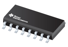
CD74AC251,
CD74ACT251 Data sheet acquired from Harris Semiconductor
SCHS246 8-Input Multiplexer, Three-State August 1998 Features Description Buffered Inputs The CD74AC251 and CD74ACT251 8-input multiplexers that
utilize the Harris Advanced CMOS Logic technology. This
multiplexer features both true (Y) and complement (Y) outputs
as well as an Output Enable (OE) input. The OE must be at a
LOW logic level to enable this device. When the OE input is
HIGH, both outputs are in the high-impedance state. When
enabled, address information on the data select inputs determines which data input is routed to the Y and Y outputs. Typical Propagation Delay
-6ns at VCC = 5V, TA = 25oC, CL = 50pF Exceeds 2kV ESD Protection MIL-STD-883, Method
3015 SCR-Latchup-Resistant CMOS Process and Circuit
Design Ordering Information Speed of Bipolar FASTв„ў/AS/S with Significantly
Reduced Power Consumption PART
NUMBER Balanced Propagation Delays AC Types Feature 1.5V to 5.5V Operation and
Balanced Noise Immunity at 30% of the Supply В±24mA Output Drive Current
-Fanout to 15 FASTв„ў ICs
-Drives 50Ω Transmission Lines Pinout TEMP.
RANGE (oC) PKG.
NO. PACKAGE CD74AC251E 0 to 70oC, -40 to 85, 16 Ld PDIP
-55 to 125 E16.3 CD74ACT251E 0 to 70oC, -40 to 85, 16 Ld PDIP
-55 to 125 E16.3 CD74AC251M 0 to 70oC, -40 to 85, 16 Ld SOIC
-55 to 125 M16.15 CD74ACT251M 0 to 70oC, -40 to 85, 16 Ld SOIC
-55 to 125 M16.15 NOTES: …
