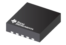
Datasheet Texas Instruments TPS61087DRCTG4 — 数据表
| 制造商 | Texas Instruments |
| 系列 | TPS61087 |
| 零件号 | TPS61087DRCTG4 |

具有强制PWM模式的18.5V,3.2A,650kHz / 1.2MHz升压DC-DC转换器10-VSON -40至85
数据表
TPS61087 650-kHz,1.2-MHz, 18.5-V Step-Up DC-DC Converter With 3.2-A Switch datasheet
PDF, 1.4 Mb, 修订版: D, 档案已发布: Dec 17, 2014
从文件中提取
价格
状态
| Lifecycle Status | Active (Recommended for new designs) |
| Manufacture's Sample Availability | Yes |
打包
| Pin | 10 |
| Package Type | DRC |
| Industry STD Term | VSON |
| JEDEC Code | S-PDSO-N |
| Package QTY | 250 |
| Carrier | SMALL T&R |
| Device Marking | PMOQ |
| Width (mm) | 3 |
| Length (mm) | 3 |
| Thickness (mm) | .9 |
| Pitch (mm) | .5 |
| Max Height (mm) | 1 |
| Mechanical Data | 下载 |
参数化
| Duty Cycle(Max) | 90 % |
| Iq(Typ) | 0.075 mA |
| Operating Temperature Range | -40 to 85 C |
| Package Group | VSON |
| Rating | Catalog |
| Regulated Outputs | 1 |
| Special Features | Enable,Frequency Synchronization,Power Good |
| Switch Current Limit(Min) | 3.2 A |
| Switch Current Limit(Typ) | 4 A |
| Switching Frequency(Max) | 1500 kHz |
| Switching Frequency(Min) | 900 kHz |
| Type | Converter |
| Vin(Max) | 6 V |
| Vin(Min) | 2.5 V |
| Vout(Max) | 18.5 V |
| Vout(Min) | 3 V |
生态计划
| RoHS | Compliant |
设计套件和评估模块
- Evaluation Modules & Boards: TPS61087EVM-317
TPS61087 Evaluation Module
Lifecycle Status: Active (Recommended for new designs)
应用须知
- Discrete Charge Pump Design (Rev. A)PDF, 190 Kb, 修订版: A, 档案已发布: Jul 16, 2010
Many applications require an auxiliary power supply in addition to a primary power supply. For example, TFT-LCD applications can require +20 V to +30 V and +10 V to +20 V. As a result of cost, board space, or inventory, a separate converter may not be appropriate for some applications. This document demonstrates a simple charge pump circuit that provides the auxiliary positive voltage using the TP - Low Cost 1W Isolated Power Supply Solution with TPS61085PDF, 175 Kb, 档案已发布: Jun 26, 2012
- AN-2020 Thermal Design By Insight, Not Hindsight (Rev. C)PDF, 568 Kb, 修订版: C, 档案已发布: Apr 23, 2013
This application report provides an in-depth discussion of thermal design. - Minimizing Ringing at the Switch Node of a Boost ConverterPDF, 201 Kb, 档案已发布: Sep 15, 2006
The application report explains how to use proper board layout and/or a snubber to reduce high-frequency ringing at the switch node of a boost converter. - Design considerations for a resistive feedback divider in a DC/DC converterPDF, 393 Kb, 档案已发布: Apr 26, 2012
- Basic Calculation of a Boost Converter's Power Stage (Rev. C)PDF, 186 Kb, 修订版: C, 档案已发布: Jan 8, 2014
This application note gives the equations to calculate the power stage of a boost converter built with an IC with integrated switch and operating in continuous conduction mode. It is not intended to give details on the functionality of a boost converter (see Reference 1) or how to compensate a converter. See the references at the end of this document if more detail is needed. - PowerPAD Thermally Enhanced Package (Rev. H)PDF, 983 Kb, 修订版: H, 档案已发布: Jul 6, 2018
- Understanding the Absolute Maximum Ratings of the SW Node (Rev. A)PDF, 755 Kb, 修订版: A, 档案已发布: Jan 13, 2012
- Extending the Soft Start Time Without a Soft Start Pin (Rev. B)PDF, 387 Kb, 修订版: B, 档案已发布: Jun 15, 2017
- QFN and SON PCB Attachment (Rev. B)PDF, 821 Kb, 修订版: B, 档案已发布: Aug 24, 2018
- IQ: What it is what it isn’t and how to use itPDF, 198 Kb, 档案已发布: Jun 17, 2011
- Performing Accurate PFM Mode Efficiency Measurements (Rev. A)PDF, 418 Kb, 修订版: A, 档案已发布: Dec 11, 2018
When performing measurements on DC-DC converters using pulse frequency modulation(PFM)or any power save mode proper care must be taken to ensure that the measurements are accurate. An accurate PFM mode efficiency measurement is critical for systems which require high efficiency at low loads such as in smart home systems tablets wearables and metering.
模型线
系列: TPS61087 (6)
- TPS61087DRCR TPS61087DRCRG4 TPS61087DRCT TPS61087DRCTG4 TPS61087DSCR TPS61087DSCT
制造商分类
- Semiconductors > Power Management > Non-isolated DC/DC Switching Regulator > Step-Up (Boost) > Boost Converter (Integrated Switch)