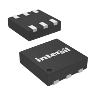
Plastic Packages for Integrated Circuits
Ultra Thin Dual Flat No-Lead Plastic Package (UTDFN)
A A E
6 B 6 LEAD ULTRA THIN DUAL FLAT NO-LEAD PLASTIC PACKAGE 4 MILLIMETERS D PIN 1
REFERENCE
2X
0.15 C
1
2X L6.1.6x1.6A 3 MIN NOMINAL MAX NOTES A 0.45 0.50 0.55 -A1 -0.05 -0.127 REF A3 0.15 C
A1 TOP VIEW
e
1.00 REF
4 6
L
CO.2 D2 SYMBOL b 0.15 0.20 0.25 -D 1.55 1.60 1.65 4 D2 0.40 0.45 0.50 -E 1.55 1.60 1.65 4 E2 0.95 1.00 1.05 -0.50 BSC e
DAP SIZE 1.30 x 0.76 L
3 1 b 6X
0.10 M C A B E2 -0.25 0.30 0.35 Rev. 1 6/06 NOTES:
1. Dimensions are in mm. Angles in degrees. BOTTOM VIEW 2. Coplanarity applies to the exposed pad as well as the terminals.
Coplanarity shall not exceed 0.08mm.
DETAIL A 6X 0.10 C 3. Warpage shall not exceed 0.10mm. 0.08 C 4. Package length/package width are considered as special
characteristics.
5. JEDEC Reference MO-229. …