Datasheet Texas Instruments OPA694 — 数据表
| 制造商 | Texas Instruments |
| 系列 | OPA694 |
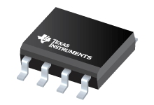
宽带,低功耗,电流反馈放大器
数据表
Wideband, Low Power, Current Feedback Operational Amplifier datasheet
PDF, 1.0 Mb, 修订版: G, 档案已发布: Jan 15, 2010
从文件中提取
价格
状态
| OPA694ID | OPA694IDBVR | OPA694IDBVT | OPA694IDBVTG4 | OPA694IDG4 | OPA694IDR | OPA694IDRG4 | |
|---|---|---|---|---|---|---|---|
| Lifecycle Status | Active (Recommended for new designs) | Active (Recommended for new designs) | Active (Recommended for new designs) | Active (Recommended for new designs) | Active (Recommended for new designs) | Active (Recommended for new designs) | Active (Recommended for new designs) |
| Manufacture's Sample Availability | Yes | Yes | Yes | Yes | No | No | No |
打包
| OPA694ID | OPA694IDBVR | OPA694IDBVT | OPA694IDBVTG4 | OPA694IDG4 | OPA694IDR | OPA694IDRG4 | |
|---|---|---|---|---|---|---|---|
| N | 1 | 2 | 3 | 4 | 5 | 6 | 7 |
| Pin | 8 | 5 | 5 | 5 | 8 | 8 | 8 |
| Package Type | D | DBV | DBV | DBV | D | D | D |
| Industry STD Term | SOIC | SOT-23 | SOT-23 | SOT-23 | SOIC | SOIC | SOIC |
| JEDEC Code | R-PDSO-G | R-PDSO-G | R-PDSO-G | R-PDSO-G | R-PDSO-G | R-PDSO-G | R-PDSO-G |
| Package QTY | 75 | 3000 | 250 | 250 | 75 | 2500 | 2500 |
| Carrier | TUBE | LARGE T&R | SMALL T&R | SMALL T&R | TUBE | LARGE T&R | LARGE T&R |
| Device Marking | OPA | BIA | BIA | BIA | 694 | 694 | OPA |
| Width (mm) | 3.91 | 1.6 | 1.6 | 1.6 | 3.91 | 3.91 | 3.91 |
| Length (mm) | 4.9 | 2.9 | 2.9 | 2.9 | 4.9 | 4.9 | 4.9 |
| Thickness (mm) | 1.58 | 1.2 | 1.2 | 1.2 | 1.58 | 1.58 | 1.58 |
| Pitch (mm) | 1.27 | .95 | .95 | .95 | 1.27 | 1.27 | 1.27 |
| Max Height (mm) | 1.75 | 1.45 | 1.45 | 1.45 | 1.75 | 1.75 | 1.75 |
| Mechanical Data | 下载 | 下载 | 下载 | 下载 | 下载 | 下载 | 下载 |
参数化
| Parameters / Models | OPA694ID | OPA694IDBVR | OPA694IDBVT | OPA694IDBVTG4 | OPA694IDG4 | OPA694IDR | OPA694IDRG4 |
|---|---|---|---|---|---|---|---|
| 2nd Harmonic, dBc | 68 | 68 | 68 | 68 | 68 | 68 | 68 |
| 3rd Harmonic, dBc | 72 | 72 | 72 | 72 | 72 | 72 | 72 |
| @ MHz | 5 | 5 | 5 | 5 | 5 | 5 | 5 |
| Acl, min spec gain, V/V | 1 | 1 | 1 | 1 | 1 | 1 | 1 |
| Additional Features | N/A | N/A | N/A | N/A | N/A | N/A | N/A |
| Architecture | Bipolar,Current FB | Bipolar,Current FB | Bipolar,Current FB | Bipolar,Current FB | Bipolar,Current FB | Bipolar,Current FB | Bipolar,Current FB |
| BW @ Acl, MHz | 1500 | 1500 | 1500 | 1500 | 1500 | 1500 | 1500 |
| CMRR(Min), dB | 55 | 55 | 55 | 55 | 55 | 55 | 55 |
| CMRR(Typ), dB | 60 | 60 | 60 | 60 | 60 | 60 | 60 |
| GBW(Typ), MHz | 1500 | 1500 | 1500 | 1500 | 1500 | 1500 | 1500 |
| Input Bias Current(Max), pA | 20000000 | 20000000 | 20000000 | 20000000 | 20000000 | 20000000 | 20000000 |
| Iq per channel(Max), mA | 6 | 6 | 6 | 6 | 6 | 6 | 6 |
| Iq per channel(Typ), mA | 5.8 | 5.8 | 5.8 | 5.8 | 5.8 | 5.8 | 5.8 |
| Number of Channels | 1 | 1 | 1 | 1 | 1 | 1 | 1 |
| Offset Drift(Typ), uV/C | 15 | 15 | 15 | 15 | 15 | 15 | 15 |
| Operating Temperature Range, C | -40 to 85 | -40 to 85 | -40 to 85 | -40 to 85 | -40 to 85 | -40 to 85 | -40 to 85 |
| Output Current(Typ), mA | 80 | 80 | 80 | 80 | 80 | 80 | 80 |
| Package Group | SOIC | SOT-23 | SOT-23 | SOT-23 | SOIC | SOIC | SOIC |
| Package Size: mm2:W x L, PKG | 8SOIC: 29 mm2: 6 x 4.9(SOIC) | 5SOT-23: 8 mm2: 2.8 x 2.9(SOT-23) | 5SOT-23: 8 mm2: 2.8 x 2.9(SOT-23) | 5SOT-23: 8 mm2: 2.8 x 2.9(SOT-23) | 8SOIC: 29 mm2: 6 x 4.9(SOIC) | 8SOIC: 29 mm2: 6 x 4.9(SOIC) | 8SOIC: 29 mm2: 6 x 4.9(SOIC) |
| Rail-to-Rail | No | No | No | No | No | No | No |
| Rating | Catalog | Catalog | Catalog | Catalog | Catalog | Catalog | Catalog |
| Slew Rate(Typ), V/us | 1700 | 1700 | 1700 | 1700 | 1700 | 1700 | 1700 |
| Total Supply Voltage(Max), +5V=5, +/-5V=10 | 12.6 | 12.6 | 12.6 | 12.6 | 12.6 | 12.6 | 12.6 |
| Total Supply Voltage(Min), +5V=5, +/-5V=10 | 7 | 7 | 7 | 7 | 7 | 7 | 7 |
| Vn at 1kHz(Typ), nV/rtHz | 2.1 | 2.1 | 2.1 | 2.1 | 2.1 | 2.1 | 2.1 |
| Vn at Flatband(Typ), nV/rtHz | 2.1 | 2.1 | 2.1 | 2.1 | 2.1 | 2.1 | 2.1 |
| Vos (Offset Voltage @ 25C)(Max), mV | 3 | 3 | 3 | 3 | 3 | 3 | 3 |
生态计划
| OPA694ID | OPA694IDBVR | OPA694IDBVT | OPA694IDBVTG4 | OPA694IDG4 | OPA694IDR | OPA694IDRG4 | |
|---|---|---|---|---|---|---|---|
| RoHS | Compliant | Compliant | Compliant | Compliant | Compliant | Compliant | Compliant |
应用须知
- RF and IF amplifiers with op ampsPDF, 177 Kb, 档案已发布: Feb 28, 2005
- Current Feedback Amplifiers: Review, Stability Analysis, and ApplicationsPDF, 53 Kb, 档案已发布: Nov 20, 2000
The majority of op amp circuits are closed-loop feedback systems that implement classical control theory analysis. Analog designers are comfortable with Voltage FeedBack (VFB) op amps in a closed-loop system and are familiar with the ideal op amp approximations feedback permit. This application bulletin will demonstrate how CFB op amps can be analyzed in a similar fashion. Once the closed-loop sim - Stabilizing Current-Feedback Op Amps While Optimizing Circuit PerformancePDF, 280 Kb, 档案已发布: Apr 28, 2004
Optimizing a circuit design with a current-feedback (CFB) op amp is a relatively straightforward task, once one understands how CFB op amps achieve stability. This application note explains a 2nd-order CFB model so that any designer can better understand the flexibility of the CFB op amp. This report also discusses stability analysis, the effects of parasitic components due to PCBs, optimization - Active filters using current-feedback amplifiersPDF, 227 Kb, 档案已发布: Feb 25, 2005
- Expanding the usability of current-feedback amplifiersPDF, 215 Kb, 档案已发布: Feb 28, 2005
- RLC Filter Design for ADC Interface Applications (Rev. A)PDF, 299 Kb, 修订版: A, 档案已发布: May 13, 2015
As high performance Analog-to-Digital Converters (ADCs) continue to improve in their performance, the last stage interface from the final amplifier into the converter inputs becomes a critical element in the system design if the full converter dynamic range is desired. This application note describes the performance and design equations for a simple passive 2nd-order filter used successfully in AD - Measuring Board Parasitics in High-Speed Analog DesignPDF, 134 Kb, 档案已发布: Jul 7, 2003
Successful circuit designs using high-speed amplifiers can depend upon understanding and identifying parasitic PCB components. Simulating a design while including PCB parasitics can protect against unpleasant production surprises. This application report discusses an easy method for measuring parasitic components in a prototype or final PC board design by using a standard oscilloscope and low freq - Noise Analysis for High Speed Op Amps (Rev. A)PDF, 256 Kb, 修订版: A, 档案已发布: Jan 17, 2005
As system bandwidths have increased an accurate estimate of the noise contribution for each element in the signal channel has become increasingly important. Many designers are not however particularly comfortable with the calculations required to predict the total noise for an op amp or in the conversions between the different descriptions of noise. Considerable inconsistency between manufactu
模型线
系列: OPA694 (7)
制造商分类
- Semiconductors> Amplifiers> Operational Amplifiers (Op Amps)> High-Speed Op Amps (>=50MHz)