Datasheet Texas Instruments CD74AC05 — 数据表
| 制造商 | Texas Instruments |
| 系列 | CD74AC05 |
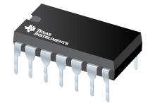
具有漏极开路输出的六边形逆变器
数据表
价格
状态
| CD74AC05E | CD74AC05EE4 | CD74AC05M | CD74AC05M96 | CD74AC05M96E4 | CD74AC05M96G4 | CD74AC05ME4 | CD74AC05MG4 | |
|---|---|---|---|---|---|---|---|---|
| Lifecycle Status | Active (Recommended for new designs) | Active (Recommended for new designs) | Active (Recommended for new designs) | Active (Recommended for new designs) | Active (Recommended for new designs) | Active (Recommended for new designs) | Active (Recommended for new designs) | Active (Recommended for new designs) |
| Manufacture's Sample Availability | No | No | Yes | No | No | No | No | Yes |
打包
| CD74AC05E | CD74AC05EE4 | CD74AC05M | CD74AC05M96 | CD74AC05M96E4 | CD74AC05M96G4 | CD74AC05ME4 | CD74AC05MG4 | |
|---|---|---|---|---|---|---|---|---|
| N | 1 | 2 | 3 | 4 | 5 | 6 | 7 | 8 |
| Pin | 14 | 14 | 14 | 14 | 14 | 14 | 14 | 14 |
| Package Type | N | N | D | D | D | D | D | D |
| Industry STD Term | PDIP | PDIP | SOIC | SOIC | SOIC | SOIC | SOIC | SOIC |
| JEDEC Code | R-PDIP-T | R-PDIP-T | R-PDSO-G | R-PDSO-G | R-PDSO-G | R-PDSO-G | R-PDSO-G | R-PDSO-G |
| Package QTY | 25 | 25 | 50 | 2500 | 2500 | 2500 | 50 | 50 |
| Carrier | TUBE | TUBE | TUBE | LARGE T&R | LARGE T&R | LARGE T&R | TUBE | TUBE |
| Device Marking | CD74AC05E | CD74AC05E | AC05M | AC05M | AC05M | AC05M | AC05M | AC05M |
| Width (mm) | 6.35 | 6.35 | 3.91 | 3.91 | 3.91 | 3.91 | 3.91 | 3.91 |
| Length (mm) | 19.3 | 19.3 | 8.65 | 8.65 | 8.65 | 8.65 | 8.65 | 8.65 |
| Thickness (mm) | 3.9 | 3.9 | 1.58 | 1.58 | 1.58 | 1.58 | 1.58 | 1.58 |
| Pitch (mm) | 2.54 | 2.54 | 1.27 | 1.27 | 1.27 | 1.27 | 1.27 | 1.27 |
| Max Height (mm) | 5.08 | 5.08 | 1.75 | 1.75 | 1.75 | 1.75 | 1.75 | 1.75 |
| Mechanical Data | 下载 | 下载 | 下载 | 下载 | 下载 | 下载 | 下载 | 下载 |
参数化
| Parameters / Models | CD74AC05E | CD74AC05EE4 | CD74AC05M | CD74AC05M96 | CD74AC05M96E4 | CD74AC05M96G4 | CD74AC05ME4 | CD74AC05MG4 |
|---|---|---|---|---|---|---|---|---|
| Bits | 8 | 8 | 8 | 8 | 8 | 8 | 8 | 8 |
| F @ Nom Voltage(Max), Mhz | 100 | 100 | 100 | 100 | 100 | 100 | 100 | 100 |
| ICC @ Nom Voltage(Max), mA | 0.04 | 0.04 | 0.04 | 0.04 | 0.04 | 0.04 | 0.04 | 0.04 |
| Operating Temperature Range, C | -55 to 125 | -55 to 125 | -55 to 125 | -55 to 125 | -55 to 125 | -55 to 125 | -55 to 125 | -55 to 125 |
| Output Drive (IOL/IOH)(Max), mA | -24/24 | -24/24 | -24/24 | -24/24 | -24/24 | -24/24 | -24/24 | -24/24 |
| Package Group | PDIP | PDIP | SOIC | SOIC | SOIC | SOIC | SOIC | SOIC |
| Package Size: mm2:W x L, PKG | See datasheet (PDIP) | See datasheet (PDIP) | 14SOIC: 52 mm2: 6 x 8.65(SOIC) | 14SOIC: 52 mm2: 6 x 8.65(SOIC) | 14SOIC: 52 mm2: 6 x 8.65(SOIC) | 14SOIC: 52 mm2: 6 x 8.65(SOIC) | 14SOIC: 52 mm2: 6 x 8.65(SOIC) | 14SOIC: 52 mm2: 6 x 8.65(SOIC) |
| Rating | Catalog | Catalog | Catalog | Catalog | Catalog | Catalog | Catalog | Catalog |
| Schmitt Trigger | No | No | No | No | No | No | No | No |
| Technology Family | AC | AC | AC | AC | AC | AC | AC | AC |
| VCC(Max), V | 5.5 | 5.5 | 5.5 | 5.5 | 5.5 | 5.5 | 5.5 | 5.5 |
| VCC(Min), V | 1.5 | 1.5 | 1.5 | 1.5 | 1.5 | 1.5 | 1.5 | 1.5 |
| Voltage(Nom), V | 1.5,3.3,5 | 1.5,3.3,5 | 1.5,3.3,5 | 1.5,3.3,5 | 1.5,3.3,5 | 1.5,3.3,5 | 1.5,3.3,5 | 1.5,3.3,5 |
| tpd @ Nom Voltage(Max), ns | 94,10.4,7.5 | 94,10.4,7.5 | 94,10.4,7.5 | 94,10.4,7.5 | 94,10.4,7.5 | 94,10.4,7.5 | 94,10.4,7.5 | 94,10.4,7.5 |
生态计划
| CD74AC05E | CD74AC05EE4 | CD74AC05M | CD74AC05M96 | CD74AC05M96E4 | CD74AC05M96G4 | CD74AC05ME4 | CD74AC05MG4 | |
|---|---|---|---|---|---|---|---|---|
| RoHS | Compliant | Compliant | Compliant | Compliant | Compliant | Compliant | Compliant | Compliant |
| Pb Free | Yes | Yes |
应用须知
- Using High Speed CMOS and Advanced CMOS in Systems With Multiple VccPDF, 43 Kb, 档案已发布: Apr 1, 1996
Though low power consumption is a feature of CMOS devices sometimes this feature does not meet a designer?s system power supply constraints. Therefore a partial system power down or multiple Vcc supplies are used to meet the needs of the system. This document shows electrostatic discharge protection circuits. It also provides circuit and bus driver examples of partial system power down and curren
模型线
系列: CD74AC05 (8)
制造商分类
- Semiconductors> Logic> Buffer/Driver/Transceiver> Inverting Buffer/Driver