Datasheet Texas Instruments 74ACT16245 — 数据表
| 制造商 | Texas Instruments |
| 系列 | 74ACT16245 |
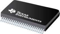
具有三态输出的16位总线收发器
数据表
16-Bit Bus Transceivers With 3-State Outputs datasheet
PDF, 737 Kb, 修订版: B, 档案已发布: Apr 1, 1996
从文件中提取
价格
状态
| 74ACT16245DGGR | 74ACT16245DGGRE4 | 74ACT16245DGGRG4 | 74ACT16245DL | 74ACT16245DLG4 | 74ACT16245DLR | 74ACT16245DLRG4 | |
|---|---|---|---|---|---|---|---|
| Lifecycle Status | Active (Recommended for new designs) | Active (Recommended for new designs) | Active (Recommended for new designs) | Active (Recommended for new designs) | Active (Recommended for new designs) | Active (Recommended for new designs) | Active (Recommended for new designs) |
| Manufacture's Sample Availability | Yes | No | No | No | No | No | No |
打包
| 74ACT16245DGGR | 74ACT16245DGGRE4 | 74ACT16245DGGRG4 | 74ACT16245DL | 74ACT16245DLG4 | 74ACT16245DLR | 74ACT16245DLRG4 | |
|---|---|---|---|---|---|---|---|
| N | 1 | 2 | 3 | 4 | 5 | 6 | 7 |
| Pin | 48 | 48 | 48 | 48 | 48 | 48 | 48 |
| Package Type | DGG | DGG | DGG | DL | DL | DL | DL |
| Industry STD Term | TSSOP | TSSOP | TSSOP | SSOP | SSOP | SSOP | SSOP |
| JEDEC Code | R-PDSO-G | R-PDSO-G | R-PDSO-G | R-PDSO-G | R-PDSO-G | R-PDSO-G | R-PDSO-G |
| Package QTY | 2000 | 2000 | 2000 | 25 | 25 | 1000 | 1000 |
| Carrier | LARGE T&R | LARGE T&R | LARGE T&R | TUBE | TUBE | LARGE T&R | LARGE T&R |
| Device Marking | ACT16245 | ACT16245 | ACT16245 | ACT16245 | ACT16245 | ACT16245 | ACT16245 |
| Width (mm) | 6.1 | 6.1 | 6.1 | 7.49 | 7.49 | 7.49 | 7.49 |
| Length (mm) | 12.5 | 12.5 | 12.5 | 15.88 | 15.88 | 15.88 | 15.88 |
| Thickness (mm) | 1.15 | 1.15 | 1.15 | 2.59 | 2.59 | 2.59 | 2.59 |
| Pitch (mm) | .5 | .5 | .5 | .635 | .635 | .635 | .635 |
| Max Height (mm) | 1.2 | 1.2 | 1.2 | 2.79 | 2.79 | 2.79 | 2.79 |
| Mechanical Data | 下载 | 下载 | 下载 | 下载 | 下载 | 下载 | 下载 |
参数化
| Parameters / Models | 74ACT16245DGGR | 74ACT16245DGGRE4 | 74ACT16245DGGRG4 | 74ACT16245DL | 74ACT16245DLG4 | 74ACT16245DLR | 74ACT16245DLRG4 |
|---|---|---|---|---|---|---|---|
| Bits | 16 | 16 | 16 | 16 | 16 | 16 | 16 |
| F @ Nom Voltage(Max), Mhz | 90 | 90 | 90 | 90 | 90 | 90 | 90 |
| ICC @ Nom Voltage(Max), mA | 0.08 | 0.08 | 0.08 | 0.08 | 0.08 | 0.08 | 0.08 |
| Operating Temperature Range, C | -40 to 85 | -40 to 85 | -40 to 85 | -40 to 85 | -40 to 85 | -40 to 85 | -40 to 85 |
| Output Drive (IOL/IOH)(Max), mA | -24/24 | -24/24 | -24/24 | -24/24 | -24/24 | -24/24 | -24/24 |
| Package Group | TSSOP | TSSOP | TSSOP | SSOP | SSOP | SSOP | SSOP |
| Package Size: mm2:W x L, PKG | 48TSSOP: 101 mm2: 8.1 x 12.5(TSSOP) | 48TSSOP: 101 mm2: 8.1 x 12.5(TSSOP) | 48TSSOP: 101 mm2: 8.1 x 12.5(TSSOP) | 48SSOP: 164 mm2: 10.35 x 15.88(SSOP) | 48SSOP: 164 mm2: 10.35 x 15.88(SSOP) | 48SSOP: 164 mm2: 10.35 x 15.88(SSOP) | 48SSOP: 164 mm2: 10.35 x 15.88(SSOP) |
| Rating | Catalog | Catalog | Catalog | Catalog | Catalog | Catalog | Catalog |
| Schmitt Trigger | No | No | No | No | No | No | No |
| Technology Family | ACT | ACT | ACT | ACT | ACT | ACT | ACT |
| VCC(Max), V | 5.5 | 5.5 | 5.5 | 5.5 | 5.5 | 5.5 | 5.5 |
| VCC(Min), V | 4.5 | 4.5 | 4.5 | 4.5 | 4.5 | 4.5 | 4.5 |
| Voltage(Nom), V | 5 | 5 | 5 | 5 | 5 | 5 | 5 |
| tpd @ Nom Voltage(Max), ns | 10.5 | 10.5 | 10.5 | 10.5 | 10.5 | 10.5 | 10.5 |
生态计划
| 74ACT16245DGGR | 74ACT16245DGGRE4 | 74ACT16245DGGRG4 | 74ACT16245DL | 74ACT16245DLG4 | 74ACT16245DLR | 74ACT16245DLRG4 | |
|---|---|---|---|---|---|---|---|
| RoHS | Compliant | Compliant | Compliant | Compliant | Compliant | Compliant | Compliant |
应用须知
- Selecting the Right Level Translation Solution (Rev. A)PDF, 313 Kb, 修订版: A, 档案已发布: Jun 22, 2004
Supply voltages continue to migrate to lower nodes to support today's low-power high-performance applications. While some devices are capable of running at lower supply nodes others might not have this capability. To haveswitching compatibility between these devices the output of each driver must be compliant with the input of the receiver that it is driving. There are several level-translati - Introduction to LogicPDF, 93 Kb, 档案已发布: Apr 30, 2015
- Implications of Slow or Floating CMOS Inputs (Rev. D)PDF, 260 Kb, 修订版: D, 档案已发布: Jun 23, 2016
- TI IBIS File Creation Validation and Distribution ProcessesPDF, 380 Kb, 档案已发布: Aug 29, 2002
The Input/Output Buffer Information Specification (IBIS) also known as ANSI/EIA-656 has become widely accepted among electronic design automation (EDA) vendors semiconductor vendors and system designers as the format for digital electrical interface data. Because IBIS models do not reveal proprietary internal processes or architectural information semiconductor vendors? support for IBIS con - CMOS Power Consumption and CPD Calculation (Rev. B)PDF, 89 Kb, 修订版: B, 档案已发布: Jun 1, 1997
Reduction of power consumption makes a device more reliable. The need for devices that consume a minimum amount of power was a major driving force behind the development of CMOS technologies. As a result CMOS devices are best known for low power consumption. However for minimizing the power requirements of a board or a system simply knowing that CMOS devices may use less power than equivale - Designing With Logic (Rev. C)PDF, 186 Kb, 修订版: C, 档案已发布: Jun 1, 1997
Data sheets which usually give information on device behavior only under recommended operating conditions may only partially answer engineering questions that arise during the development of systems using logic devices. However information is frequently needed regarding the behavior of the device outside the conditions in the data sheet. Such questions might be:?How does a bus driver behave w - Using High Speed CMOS and Advanced CMOS in Systems With Multiple VccPDF, 43 Kb, 档案已发布: Apr 1, 1996
Though low power consumption is a feature of CMOS devices sometimes this feature does not meet a designer?s system power supply constraints. Therefore a partial system power down or multiple Vcc supplies are used to meet the needs of the system. This document shows electrostatic discharge protection circuits. It also provides circuit and bus driver examples of partial system power down and curren
模型线
系列: 74ACT16245 (7)
制造商分类
- Semiconductors> Logic> Buffer/Driver/Transceiver> Standard Transceiver