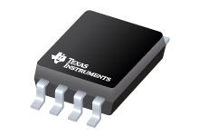
SN74LVC2T45-Q1 www.ti.com SCES818 – SEPTEMBER 2010 DUAL-BIT DUAL-SUPPLY BUS TRANSCEIVER
WITH CONFIGURABLE VOLTAGE TRANSLATION AND 3-STATE OUTPUTS
Check for Samples: SN74LVC2T45-Q1 FEATURES 1 Qualified for Automotive Applications
Fully Configurable Dual-Rail Design Allows
Each Port to Operate Over the Full 1.65-V to
5.5-V Power-Supply Range
VCC Isolation Feature – If Either VCC Input Is at
GND, Both Ports Are in the High-Impedance
State
DIR Input Circuit Referenced to VCCA
Low Power Consumption, 10-mA Max ICC
В±24-mA Output Drive at 3.3 V
Ioff Supports Partial-Power-Down Mode
Operation
Max Data Rates
– 420 Mbps (3.3-V to 5-V Translation) – 210 Mbps (Translate to 3.3 V)
– 140 Mbps (Translate to 2.5 V)
– 75 Mbps (Translate to 1.8 V) DESCRIPTION/ORDERING INFORMATION
This dual-bit noninverting bus transceiver uses two separate configurable power-supply rails. The A port is
designed to track VCCA. VCCA accepts any supply voltage from 1.65 V to 5.5 V. The B port is designed to track
VCCB. VCCB accepts any supply voltage from 1.65 V to 5.5 V. This allows for universal low-voltage bidirectional
translation between any of the 1.8-V, 2.5-V, 3.3-V, and 5-V voltage nodes.
The SN74LVC2T45-Q1 is designed for asynchronous communication between two data buses. The logic levels …