Datasheet Texas Instruments OPA453 — 数据表
| 制造商 | Texas Instruments |
| 系列 | OPA453 |
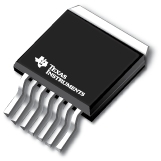
80V,50mA运算放大器
数据表
OPA452, 453: 80V, 50mA Operational Amplifiers datasheet
PDF, 917 Kb, 修订版: C, 档案已发布: Nov 10, 2003
从文件中提取
价格
状态
| OPA453FA | OPA453FAKTWT | OPA453TA | OPA453TA-1 | OPA453TA-1G3 | OPA453TAG3 | |
|---|---|---|---|---|---|---|
| Lifecycle Status | Obsolete (Manufacturer has discontinued the production of the device) | Active (Recommended for new designs) | Active (Recommended for new designs) | Active (Recommended for new designs) | Active (Recommended for new designs) | Active (Recommended for new designs) |
| Manufacture's Sample Availability | Yes | Yes | No | Yes | No | No |
打包
| OPA453FA | OPA453FAKTWT | OPA453TA | OPA453TA-1 | OPA453TA-1G3 | OPA453TAG3 | |
|---|---|---|---|---|---|---|
| N | 1 | 2 | 3 | 4 | 5 | 6 |
| Pin | 7 | 7 | 7 | 7 | 7 | 7 |
| Package Type | KTW | KTW | KC | KVT | KVT | KC |
| Industry STD Term | TO-263 | TO-263 | TO-220 | TO-220 | TO-220 | TO-220 |
| JEDEC Code | R-PSFM-G | R-PSFM-G | R-PSFM-T | R-PZFM-T | R-PZFM-T | R-PSFM-T |
| Width (mm) | 8.89 | 8.89 | 8.38 | 8.34 | 8.34 | 8.38 |
| Length (mm) | 10.1 | 10.1 | 10.17 | 10.16 | 10.16 | 10.17 |
| Thickness (mm) | 4.44 | 4.44 | 4.58 | 4.6 | 4.6 | 4.58 |
| Pitch (mm) | 1.27 | 1.27 | 1.27 | 1.27 | 1.27 | 1.27 |
| Max Height (mm) | 4.65 | 4.65 | 4.7 | 4.7 | 4.7 | 4.7 |
| Mechanical Data | 下载 | 下载 | 下载 | 下载 | 下载 | 下载 |
| Package QTY | 250 | 50 | 50 | 50 | 50 | |
| Carrier | SMALL T&R | TUBE | TUBE | TUBE | TUBE | |
| Device Marking | OPA453F | OPA453T | OPA453T | OPA453T | OPA453T |
参数化
| Parameters / Models | OPA453FA | OPA453FAKTWT | OPA453TA | OPA453TA-1 | OPA453TA-1G3 | OPA453TAG3 |
|---|---|---|---|---|---|---|
| Additional Features | Decompensated | Decompensated | Decompensated | Decompensated | Decompensated | Decompensated |
| Approx. Price (US$) | 2.90 | 1ku | |||||
| Architecture | FET | FET | FET | FET | FET | FET |
| CMRR(Min), dB | 86 | 86 | 86 | 86 | 86 | |
| CMRR(Min)(dB) | 86 | |||||
| CMRR(Typ), dB | 94 | 94 | 94 | 94 | 94 | |
| CMRR(Typ)(dB) | 94 | |||||
| GBW(Typ), MHz | 7.5 | 7.5 | 7.5 | 7.5 | 7.5 | |
| GBW(Typ)(MHz) | 7.5 | |||||
| Input Bias Current(Max), pA | 100 | 100 | 100 | 100 | 100 | |
| Input Bias Current(Max)(pA) | 100 | |||||
| Iq per channel(Max), mA | 6.5 | 6.5 | 6.5 | 6.5 | 6.5 | |
| Iq per channel(Max)(mA) | 6.5 | |||||
| Iq per channel(Typ), mA | 5.5 | 5.5 | 5.5 | 5.5 | 5.5 | |
| Iq per channel(Typ)(mA) | 5.5 | |||||
| Number of Channels | 1 | 1 | 1 | 1 | 1 | |
| Number of Channels(#) | 1 | |||||
| Offset Drift(Typ), uV/C | 5 | 5 | 5 | 5 | 5 | |
| Offset Drift(Typ)(uV/C) | 5 | |||||
| Operating Temperature Range, C | -40 to 125 | -40 to 125 | -40 to 125 | -40 to 125 | -40 to 125 | |
| Operating Temperature Range(C) | -40 to 125 | |||||
| Output Current(Typ), mA | 50 | 50 | 50 | 50 | 50 | |
| Output Current(Typ)(mA) | 50 | |||||
| Package Group | DDPAK/TO-263 | DDPAK/TO-263 | TO-220 | TO-220 | TO-220 | TO-220 |
| Package Size: mm2:W x L, PKG | 7DDPAK/TO-263: 154 mm2: 15.24 x 10.1(DDPAK/TO-263) | See datasheet (TO-220) | See datasheet (TO-220) | See datasheet (TO-220) | See datasheet (TO-220) | |
| Package Size: mm2:W x L (PKG) | See datasheet (TO-220) | |||||
| Rail-to-Rail | No | No | No | No | No | No |
| Rating | Catalog | Catalog | Catalog | Catalog | Catalog | Catalog |
| Slew Rate(Typ), V/us | 23 | 23 | 23 | 23 | 23 | |
| Slew Rate(Typ)(V/us) | 23 | |||||
| Total Supply Voltage(Max), +5V=5, +/-5V=10 | 80 | 80 | 80 | 80 | 80 | |
| Total Supply Voltage(Max)(+5V=5, +/-5V=10) | 80 | |||||
| Total Supply Voltage(Min), +5V=5, +/-5V=10 | 20 | 20 | 20 | 20 | 20 | |
| Total Supply Voltage(Min)(+5V=5, +/-5V=10) | 20 | |||||
| Vos (Offset Voltage @ 25C)(Max), mV | 3 | 3 | 3 | 3 | 3 | |
| Vos (Offset Voltage @ 25C)(Max)(mV) | 3 |
生态计划
| OPA453FA | OPA453FAKTWT | OPA453TA | OPA453TA-1 | OPA453TA-1G3 | OPA453TAG3 | |
|---|---|---|---|---|---|---|
| RoHS | Not Compliant | Compliant | Compliant | Compliant | Compliant | Compliant |
| Pb Free | No |
应用须知
- Power Amplifier Stress and Power Handling LimitationsPDF, 55 Kb, 档案已发布: Sep 27, 2000
To achieve reliable power amplifier designs you must consider the stress on the amplifier compared to its power handling limitations. Power handling limits are specified by the Safe Operating Area (SOA) curves of the power amp. Stress on the amplifier depends on amplifier load and signal conditions which can be evaluated with straightforward techniques.
模型线
系列: OPA453 (6)
制造商分类
- Semiconductors> Amplifiers> Operational Amplifiers (Op Amps)> Power Op Amps