Datasheet Texas Instruments OPA301 — 数据表
| 制造商 | Texas Instruments |
| 系列 | OPA301 |
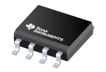
低噪声,高速,16位准确度CMOS运算放大器
数据表
Low-Noise, High-Speed,16-Bit Accurate, CMOS Operational Amplifier datasheet
PDF, 1.2 Mb, 修订版: D, 档案已发布: Jun 13, 2007
从文件中提取
价格
状态
| OPA301AID | OPA301AIDBVR | OPA301AIDBVT | OPA301AIDBVTG4 | OPA301AIDG4 | OPA301AIDR | OPA301AIDRG4 | |
|---|---|---|---|---|---|---|---|
| Lifecycle Status | Active (Recommended for new designs) | Active (Recommended for new designs) | Active (Recommended for new designs) | Active (Recommended for new designs) | Active (Recommended for new designs) | Active (Recommended for new designs) | Active (Recommended for new designs) |
| Manufacture's Sample Availability | No | No | No | No | No | No | No |
打包
| OPA301AID | OPA301AIDBVR | OPA301AIDBVT | OPA301AIDBVTG4 | OPA301AIDG4 | OPA301AIDR | OPA301AIDRG4 | |
|---|---|---|---|---|---|---|---|
| N | 1 | 2 | 3 | 4 | 5 | 6 | 7 |
| Pin | 8 | 5 | 5 | 5 | 8 | 8 | 8 |
| Package Type | D | DBV | DBV | DBV | D | D | D |
| Industry STD Term | SOIC | SOT-23 | SOT-23 | SOT-23 | SOIC | SOIC | SOIC |
| JEDEC Code | R-PDSO-G | R-PDSO-G | R-PDSO-G | R-PDSO-G | R-PDSO-G | R-PDSO-G | R-PDSO-G |
| Package QTY | 75 | 3000 | 250 | 250 | 75 | 2500 | 2500 |
| Carrier | TUBE | LARGE T&R | SMALL T&R | SMALL T&R | TUBE | LARGE T&R | LARGE T&R |
| Device Marking | OPA | AUP | AUP | AUP | OPA | OPA | 301A |
| Width (mm) | 3.91 | 1.6 | 1.6 | 1.6 | 3.91 | 3.91 | 3.91 |
| Length (mm) | 4.9 | 2.9 | 2.9 | 2.9 | 4.9 | 4.9 | 4.9 |
| Thickness (mm) | 1.58 | 1.2 | 1.2 | 1.2 | 1.58 | 1.58 | 1.58 |
| Pitch (mm) | 1.27 | .95 | .95 | .95 | 1.27 | 1.27 | 1.27 |
| Max Height (mm) | 1.75 | 1.45 | 1.45 | 1.45 | 1.75 | 1.75 | 1.75 |
| Mechanical Data | 下载 | 下载 | 下载 | 下载 | 下载 | 下载 | 下载 |
参数化
| Parameters / Models | OPA301AID | OPA301AIDBVR | OPA301AIDBVT | OPA301AIDBVTG4 | OPA301AIDG4 | OPA301AIDR | OPA301AIDRG4 |
|---|---|---|---|---|---|---|---|
| 2nd Harmonic, dBc | 75 | 75 | 75 | 75 | 75 | 75 | 75 |
| 3rd Harmonic, dBc | 79 | 79 | 79 | 79 | 79 | 79 | 79 |
| @ MHz | 1 | 1 | 1 | 1 | 1 | 1 | 1 |
| Acl, min spec gain, V/V | 1 | 1 | 1 | 1 | 1 | 1 | 1 |
| Additional Features | Shutdown | Shutdown | Shutdown | Shutdown | Shutdown | Shutdown | Shutdown |
| Architecture | CMOS,Voltage FB | CMOS,Voltage FB | CMOS,Voltage FB | CMOS,Voltage FB | CMOS,Voltage FB | CMOS,Voltage FB | CMOS,Voltage FB |
| BW @ Acl, MHz | 150 | 150 | 150 | 150 | 150 | 150 | 150 |
| CMRR(Min), dB | 66 | 66 | 66 | 66 | 66 | 66 | 66 |
| CMRR(Typ), dB | 80 | 80 | 80 | 80 | 80 | 80 | 80 |
| GBW(Typ), MHz | 150 | 150 | 150 | 150 | 150 | 150 | 150 |
| Input Bias Current(Max), pA | 5 | 5 | 5 | 5 | 5 | 5 | 5 |
| Iq per channel(Max), mA | 12 | 12 | 12 | 12 | 12 | 12 | 12 |
| Iq per channel(Typ), mA | 9.5 | 9.5 | 9.5 | 9.5 | 9.5 | 9.5 | 9.5 |
| Number of Channels | 1 | 1 | 1 | 1 | 1 | 1 | 1 |
| Offset Drift(Typ), uV/C | 2.5 | 2.5 | 2.5 | 2.5 | 2.5 | 2.5 | 2.5 |
| Operating Temperature Range, C | -40 to 125 | -40 to 125 | -40 to 125 | -40 to 125 | -40 to 125 | -40 to 125 | -40 to 125 |
| Output Current(Typ), mA | 70 | 70 | 70 | 70 | 70 | 70 | 70 |
| Package Group | SOIC | SOT-23 | SOT-23 | SOT-23 | SOIC | SOIC | SOIC |
| Package Size: mm2:W x L, PKG | 8SOIC: 29 mm2: 6 x 4.9(SOIC) | 5SOT-23: 8 mm2: 2.8 x 2.9(SOT-23) | 5SOT-23: 8 mm2: 2.8 x 2.9(SOT-23) | 5SOT-23: 8 mm2: 2.8 x 2.9(SOT-23) | 8SOIC: 29 mm2: 6 x 4.9(SOIC) | 8SOIC: 29 mm2: 6 x 4.9(SOIC) | 8SOIC: 29 mm2: 6 x 4.9(SOIC) |
| Rail-to-Rail | In to V-,Out | In to V-,Out | In to V-,Out | In to V-,Out | In to V-,Out | In to V-,Out | In to V-,Out |
| Rating | Catalog | Catalog | Catalog | Catalog | Catalog | Catalog | Catalog |
| Slew Rate(Typ), V/us | 80 | 80 | 80 | 80 | 80 | 80 | 80 |
| Total Supply Voltage(Max), +5V=5, +/-5V=10 | 5.5 | 5.5 | 5.5 | 5.5 | 5.5 | 5.5 | 5.5 |
| Total Supply Voltage(Min), +5V=5, +/-5V=10 | 2.7 | 2.7 | 2.7 | 2.7 | 2.7 | 2.7 | 2.7 |
| Vn at 1kHz(Typ), nV/rtHz | 3 | 3 | 3 | 3 | 3 | 3 | 3 |
| Vn at Flatband(Typ), nV/rtHz | 3 | 3 | 3 | 3 | 3 | 3 | 3 |
| Vos (Offset Voltage @ 25C)(Max), mV | 5 | 5 | 5 | 5 | 5 | 5 | 5 |
生态计划
| OPA301AID | OPA301AIDBVR | OPA301AIDBVT | OPA301AIDBVTG4 | OPA301AIDG4 | OPA301AIDR | OPA301AIDRG4 | |
|---|---|---|---|---|---|---|---|
| RoHS | Compliant | Compliant | Compliant | Compliant | Compliant | Compliant | Compliant |
应用须知
- High-Voltage Signal Conditioning for Low Voltage ADCsPDF, 135 Kb, 档案已发布: Jun 15, 2004
Analog designers are frequently required to develop circuits that convert high-voltage signals to levels acceptable for low-voltage data converters. This paper describes several solutions for this common task using modern amplifiers and typical power supplies. Five examples of conditioning ±10V bipolar signals for low-voltage single-rail analog-to-digital converters(ADCs) are presented: - High-Voltage Signal Conditioning for Differential ADCsPDF, 125 Kb, 档案已发布: Jun 14, 2004
Analog designers are frequently required to convert high-voltage signals to levels acceptable to low-voltage data converters with differential inputs. This paper describes solutions for this common task using modern amplifiers and typical power supplies. Three examples of conditioning В±10V bipolar signals for low-voltage analog-to-digital converters (ADCs) are shown: a single-supply design, - Tuning in AmplifiersPDF, 44 Kb, 档案已发布: Oct 2, 2000
Have you ever had the experience of designing an analog gain block with an amplifier that is specified to be unity gain stable only to find that it is oscillating out of control in your circuit? Or have you ever replaced a stable voltage feedback amplifier with a current feedback amplifier to find that the current feedback amplifier immediately oscillates when placed in the amplifier socket? Oscil - Single-Supply Operation of Operational AmplifiersPDF, 77 Kb, 档案已发布: Oct 2, 2000
Operation of op amps from single supply voltages is useful when negative supply voltages are not available. Furthermore, certain applications using high voltage and high current op amps can derive important benefits from single supply operation. - Op Amp Performance AnalysisPDF, 76 Kb, 档案已发布: Oct 2, 2000
This bulletin reflects the analysis power gained through knowledge of an op amp circuit's feedback factor. Feedback dictates the performance of an op amp both in function and in quality. The major specifications of the amplifier descibe an open-loop device awaiting feedback direction of the end circuit's function. Just how well the amplifier performs the function reflects through the feedback inte
模型线
系列: OPA301 (7)
制造商分类
- Semiconductors> Amplifiers> Operational Amplifiers (Op Amps)> High-Speed Op Amps (>=50MHz)